| Home |
NOTE: |
The procedure on this web page was written specifically for the IBM 5150 motherboard. |
NOTE: |
This procedure assumes that the problem is 'permanent', not intermittent. |
| Step 1.1 | Verify that an IBM BIOS ROM is fitted. For the IBM 5150, these are shown at here. |
| Note: | If you like, you can use Ruud's Diagnostic ROM in place of the IBM BIOS ROM, because it too has EA as the first byte of the reset vector. If you like, you can use the Supersoft/Landmark Diagnostic ROM in place of the IBM BIOS ROM, because it too has EA as the first byte of the reset vector. |
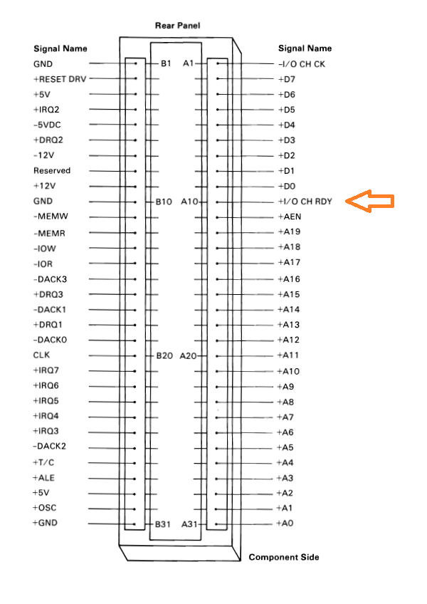
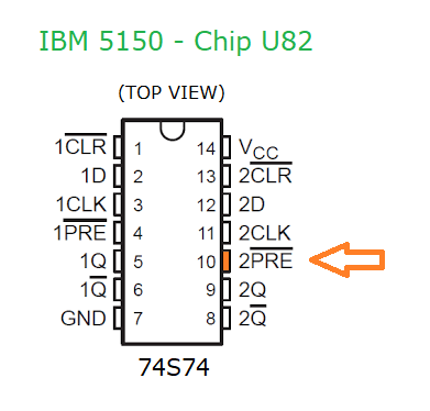
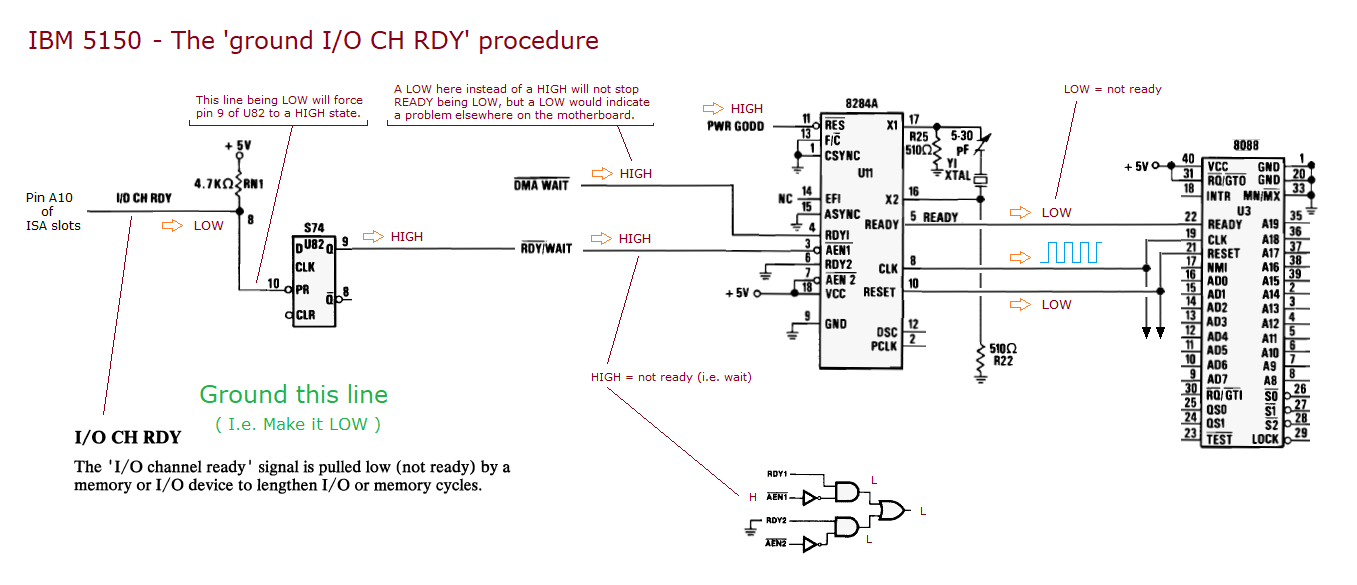
| Step 2.1 | With power off, ground the I/O CH RDY line. On the IBM 5150, following are some places where you can ground I/O CH RDY: 1. Pin A10 of an ISA slot - see here. 2. Pin 10 of chip U82 - see here. How you do the grounding is up to you, as long as it is reliable. What I use is shown at here. I use that to connect pins 10 and 7 of U82 together (i.e. grounding pin 10). This grounding needs to remain in place for all of the following steps. |
| Step 3.1 | Power on the motherboard. |
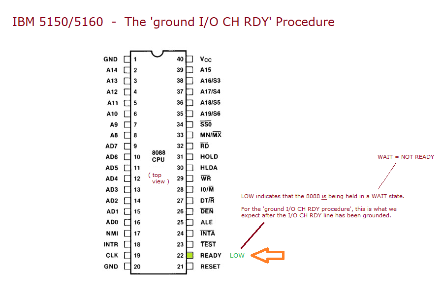
| Step 3.2 | Verify that the READY pin, pin 22, of the 8088 CPU is LOW - see here. If not LOW, use the diagram at here to see if you can work out why it is not LOW. |
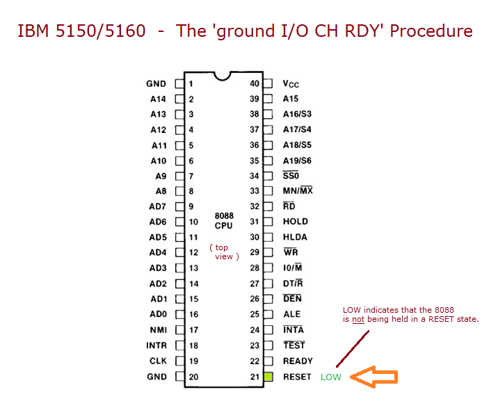
| Step 3.3 | Verify that the RESET pin, pin 21, of the 8088 CPU is LOW - see here. If not LOW, use the diagram at here to see if you can work out why it is not LOW. |
| Note: | On pin 22 (READY pin), if your logic probe is showing activity (the pulse LED is flashing) or your oscilloscope is showing activity, then something is wrong. Step 2 should result in pin 22 being continously LOW. |
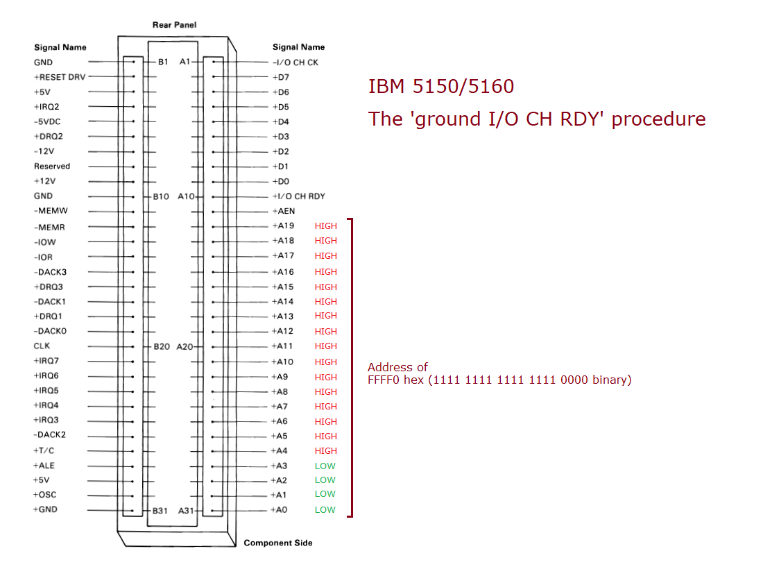
| Step 4.1 | On the address pins (A19 to A0) of an ISA slot, expect to measure the address of FFFF0 hex (1111 1111 1111 1111 0000 binary). See here. |
| Note: | If you do not measure FFFF0, it may seem logical to you to go visit the source, the 8088 CPU, and see whether or not FFFF0 is on the address pins of the 8088. For the 8088, that is only partially valid. More information is in note 1 below. |
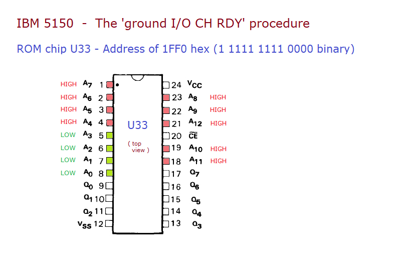
| Step 5.1 | On the address pins (A12 to A0) of ROM chip U33, expect to measure the address of 1FF0 hex (1 1111 1111 0000 binary). See here. |
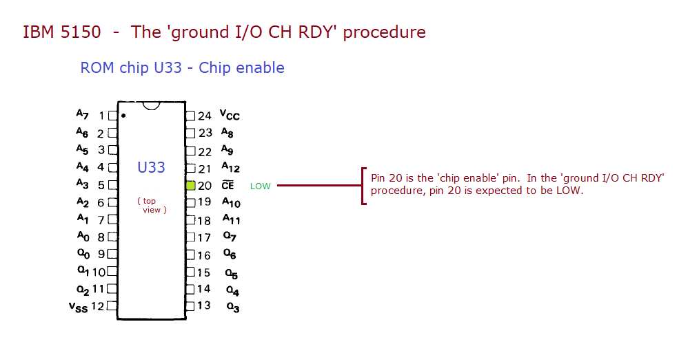
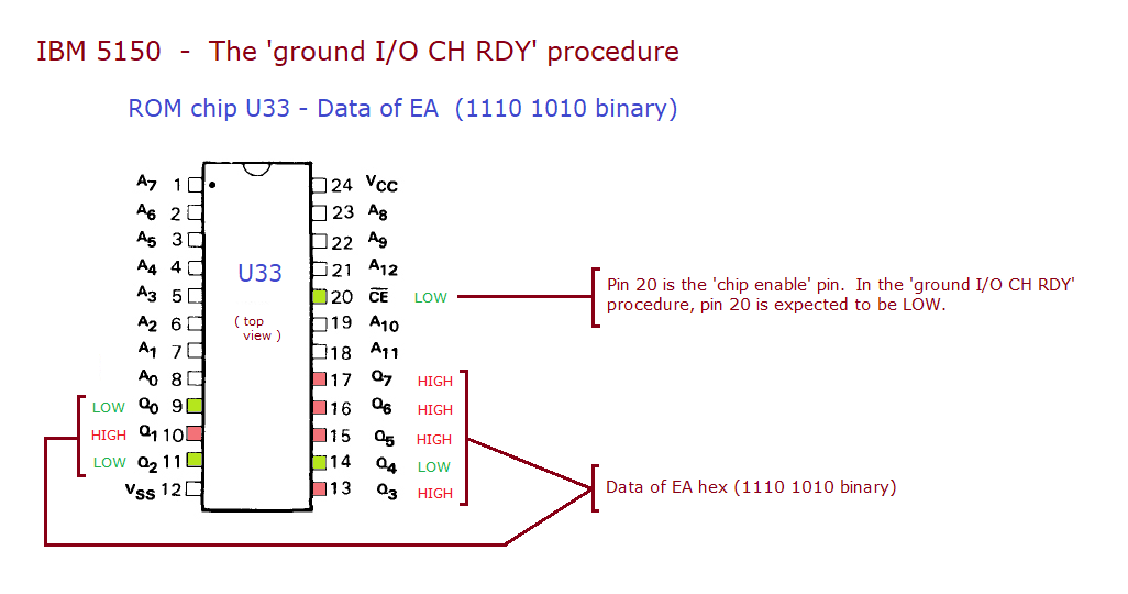
| Step 6.1 | Verify that pin 20 (/CE) of ROM chip U33 is LOW. See here. |
| Step 7.1 | On the data pins (D7 to D0) (Q7 to Q0) of ROM chip U33, expect to measure the data of EA hex (1110 1010 binary). See here. |
| Note: | If you see the data of EA coming out of the IBM BIOS ROM chip, that does not mean that the chip is 100% good. EA is just one byte of many in the ROM. There could be corrupted bytes somewhere in the ROM. Maybe the ROM has an addressing problem. The IBM BIOS ROM chip would still be under suspicion. |
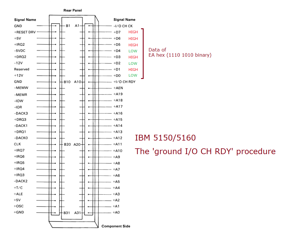
| Step 8.1 | On the data pins (D7 to D0) of an ISA slot, expect to measure the data of EA hex (1110 1010 binary). See here. |
| Step 9.1 | On the AD pins (AD7 to AD0) of the 8088 CPU, expect to measure the data of EA hex (1110 1010 binary). See here. |
| Step 10.1 | Power off. |
| Step 10.2 | Replace the IBM BIOS ROM with a suitable EPROM that contains 00 hex at every address. If you are going to program/burn your own EPROM, all-00 data for the EPROM is available at here. An alternate option is modify the IBM BIOS ROM code so that 00 is in place of the EA at the reset vector. See here for EPROM's and adapters suitable for the IBM 5150. |
| Step 10.3 | Power on. |
| Step 10.4 | On the AD pins (AD7 to AD0) of the 8088 CPU, expect to measure the data of 00 hex (0000 0000 binary). |
| Note: | Taking the shortcut of measuring this on the ISA slot is only doing half the job. The problem could be between the ISA slot and the CPU. |
| Step 11.1 | Power off. |
| Step 11.2 | Replace the IBM BIOS ROM with a suitable EPROM that contains FF hex at every address. If you are going to program/burn your own EPROM, all-FF data for the EPROM is available at here. An alternate option is modify the IBM BIOS ROM code so that FF is in place of the EA at the reset vector. See here for EPROM's and adapters suitable for the IBM 5150. |
| Step 11.3 | Power on. |
| Step 11.4 | On the AD pins (AD7 to AD0) of the 8088 CPU, expect to measure the data of FF hex (1111 1111 binary). |
| Note: | Taking the shortcut of measuring this on the ISA slot is only doing half the job. The problem could be between the ISA slot and the CPU. |
| Step 12.1 | Power off. |
| Step 12.2 | Replace the IBM BIOS ROM with a suitable EPROM that contains 55 hex at every address. If you are going to program/burn your own EPROM, all-55 data for the EPROM is available at here. An alternate option is modify the IBM BIOS ROM code so that 55 is in place of the EA at the reset vector. See here for EPROM's and adapters suitable for the IBM 5150. |
| Step 12.3 | Power on. |
| Step 12.4 | On the AD pins (AD7 to AD0) of the 8088 CPU, expect to measure the data of 55 hex (01010101 binary). |
| Note: | Taking the shortcut of measuring this on the ISA slot is only doing half the job. The problem could be between the ISA slot and the CPU. |
| Step 13.1 | Power off. |
| Step 13.2 | Replace the IBM BIOS ROM with a suitable EPROM that contains AA hex at every address. If you are going to program/burn your own EPROM, all-AA data for the EPROM is available at here. An alternate option is modify the IBM BIOS ROM code so that AA is in place of the EA at the reset vector. See here for EPROM's and adapters suitable for the IBM 5150. |
| Step 13.3 | Power on. |
| Step 13.4 | On the AD pins (AD7 to AD0) of the 8088 CPU, expect to measure the data of AA hex (10101010 binary). |
| Note: | Taking the shortcut of measuring this on the ISA slot is only doing half the job. The problem could be between the ISA slot and the CPU. |
| Note 1 | Reference diagram at here. • The pins on the 8088 that carry A19 to A16 are shared-function pins. Sometimes the 8088 outputs A19 to A16 of an address on them, and sometimes the pins contain status information. • The pins on the 8088 that carry A7 to A0 are shared-function pins. Sometimes the 8088 outputs A7 to A0 of an address on them, and sometimes the pins are the 8088's data pins. • When the aforementioned pins were acting as address pins, certain circuitry instructed chips U7, U9 and U10 to latch (capture) the complete address. • In this procedure, it is invalid to examine these shared-function pins for an address. • It is valid though to examine the other address pins, A15 to A8, on the 8088. Those pins should all be HIGH. |