| Home |
| 1. | User turns on power supply. |
| 2. | Motherboard receives +5 volts from the power supply. |
| 3. | Also received from the power supply is the POWER GOOD signal, a digital signal of TTL levels, which at this time, is low. <----- Important: At this time, the signal is LOW |
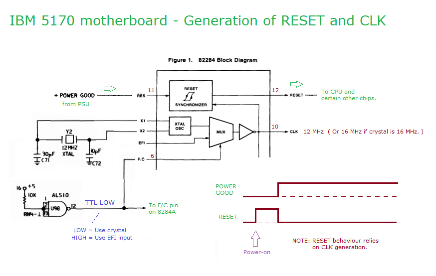
| 4. | Refer to here and here. On the motherboard, the 82284 chip generates a 16 MHz clock signal (12 MHz for the type 1 and type 2 motherboards) for the 80286 CPU and the 82288 bus controller chip. (And optional 80287 NPU, if fitted.) |
| 5. | Diagram at here. Because the POWER GOOD signal is low, the motherboard's 82284 chip takes the motherboard's RESET line high. Per here, various chips on the motherboard (including the 80286 CPU) are held in a reset state. |
| 6. | Later, when all voltages from the power supply are within specification, the power supply takes the POWER GOOD line high. |
| 7. | Diagram at here. When the 82284 chip sees the power supply's POWER GOOD signal go high, it takes the motherboard's RESET line from high to low. As a result, chips are taken out of the reset state. |
| 8. | When the 80286 CPU leaves the reset state (see note 1 below), it starts execution at address FFFFF0 (16 bytes below 16 MB). In the IBM 5170, that address corresponds to an address in the motherboard's BIOS ROM set. See note 2. |
|
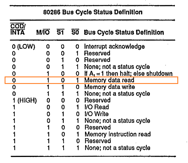
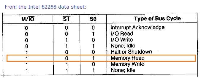
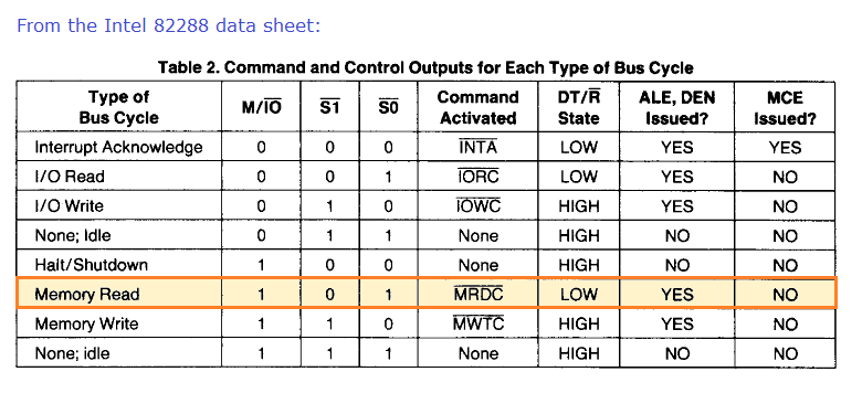
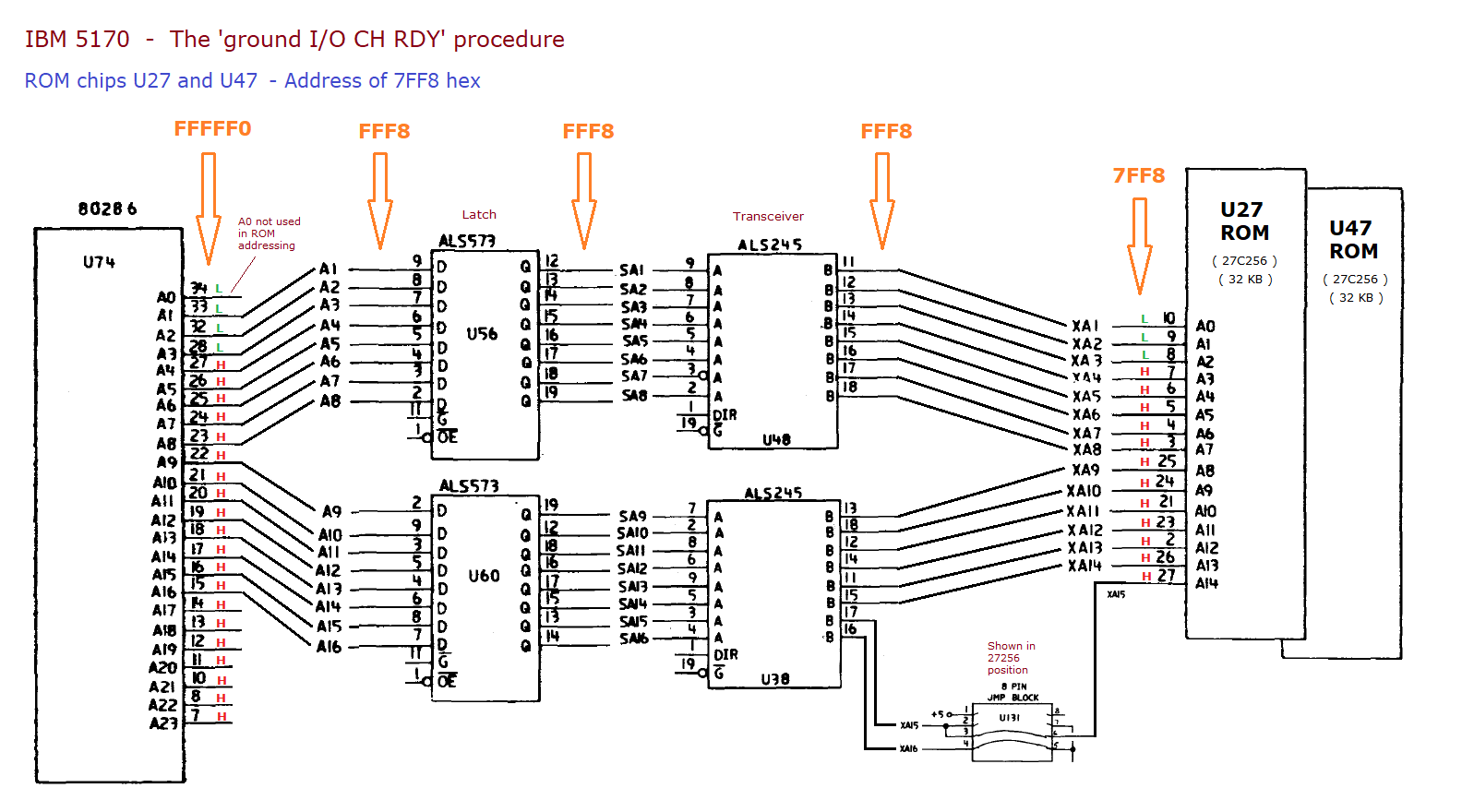
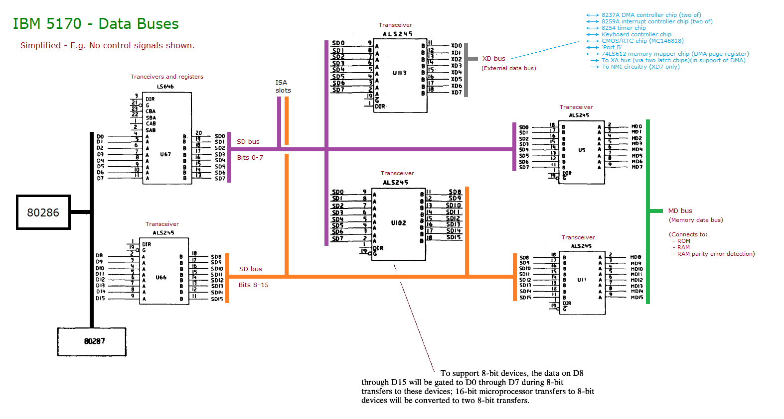
Basically (repeat: basically), the read of address FFFFF0 goes something like: - 80286 starts a 'Memory data read' bus cycle. - 80286 sets four status pins (COD/INTA, M/IO, S1 and S0) to indicate to certain other chips that a 'Memory data read' bus cycle is in progress - see here. - The 82288 chip (receives M/IO, S1 and S0) starts a 'Memory read' bus cycle - see here. - Acordingly, the 82288 chip asserts its /MRDC output pin - see here. - - The 80286 outputs address FFFFF0 onto the address bus (A23 to A0). - Per here, that address ends up being address 7FF8 on ROM chips U27 and U47. - - Certain circuitry establishes that a read of motherboard address FFFFF0 corresponds to ROM chips U27 and U47, and accordingly, asserts the two enable pins (20 and 22) on ROM chips U27 and U47 - see here. - As a result, ROM chips U27 and U47 output the data they have at address 7FF8 onto the memory data bus - see here. - - Certain circuitry directs the data on the memory data bus through to the data bus - see here. - The 80286 reads the data bus. BTW. If you have a logic probe, you can see that for yourself via the procedure at here. |
|
| 9. | Starting at address 7FF8 in the ROM's are five bytes, which together form a jump instruction to the start of the BIOS' power-on self test (POST). |
| 10. | The POST executes. |
|
If an ISA POST card is fitted, various POST codes will be sent to the ISA POST card as the POST progresses. |
| Note 1 | The data sheet for the Intel 80286 indicates that there is minimum period in which the 80286 needs to be held in a reset state for. That minimum period is 16 clock cycles, which in the IBM 5170, equates to about 2.67 ms for the 6 MHz version of the IBM 5170, and 2 ms for the 8 MHz version of the IBM 5170. |
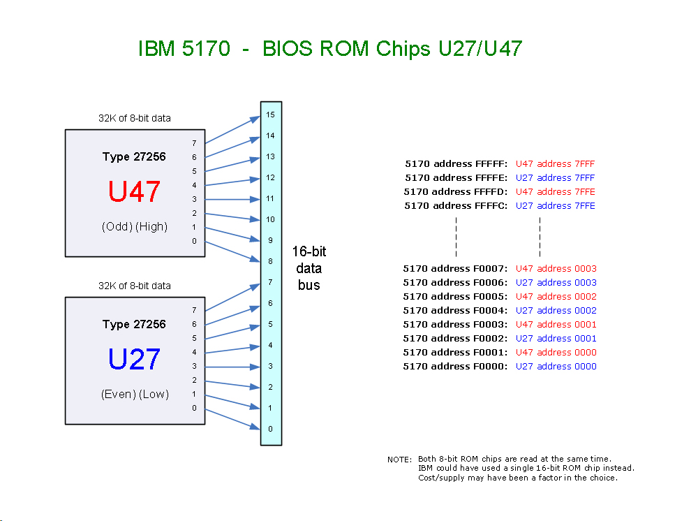
| Note 2 | A memory map of the IBM 5170 is shown on page 1-8 of the IBM document at here. As can be seen, the motherboard BIOS ROM set (U27/U47 plus optional U17/U37) not only appears in the 128 KB of address space immediately before the 1 MB address mark, it also appears in the 128 KB of address space immediately before the 16 MB address mark. |